###Simple MIPS Assembly Program initialize registers $S0 and $S1 with the decimal values 44 and -37 respectively. Use a register instruction to add these values together and store the result in $S2. Finally you will write an instruction that will store $S2 to the hexadecimal memory address x54.
# $s0 = a
 addi $s0, $0, 44   # a = 44

# $s1 = b
 addi $s1, $0, -37   # a = -37

# a + b = c
 add $s2, $s0, $s1      # c = $s2

# store c
 sw $s2, 0x54($0)       # c => 0x54
###Machine Code
| Instruction | op | rs | rt | immediate | Hex Code |
|---|---|---|---|---|---|
addi $s0, $0, 44 |
001000 | 00000 | 10000 | 0000000000101100 | 0x2010002C |
addi $s1, $0, -37 |
001000 | 00000 | 10001 | 1111111111011011 | 0x2011FFDB |
| Instruction | op | rs | rt | rd | shamt | funct | Hex Code |
|---|---|---|---|---|---|---|---|
add $s2, $s0, $s1 |
000000 | 00000 | 10001 | 10011 | 00000 | 100000 | 0x02119020 |
| Instruction | op | rs | rt | immediate | Hex Code |
|---|---|---|---|---|---|
sw $s2, 0x54($0) |
101011 | 00000 | 10010 | 0000000001010100 | 0xAC120054 |
######Simulation The given waveform file initially did not work with my created testbench. Looking in the waveform file I noticed in the XML that the filepaths which referenced the desired processes used the name "mips_tb" as the name for the testbench.
<wvobject fp_name="/mips_tb/uut/dp/rf/wd3" type="array" db_ref_id="1">I made a new testbench with this name and the simulation worked! (I also sent an email to the class explaining this fix)
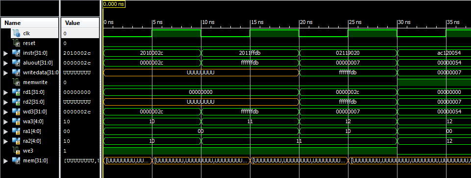
loking at the waveform the first instruction is seen "2010002c" this should add the immediate 44 into $S1, 0x2C (44) can be seen in aluout indicating the operation was sucessfully completed in the ALU. The next instruction is correctly seen as "2011ffdb". This shouls load -37 in $s1. the ALU out is ffffffdb which is the two's compliment for -37 indicating sucess. 44 + -37 = 7 so after the next operation a 7 should be seen in the aluout which is there so the add instruction was sucessfull. finally the sw instriction should have wrote the data (7), the signal writedata is 7 on the last instruction so sucess again.
###Modify the MIPS single-cycle processor by adding the ori instruction
####Schematic The modification to the diagram can be seen below.
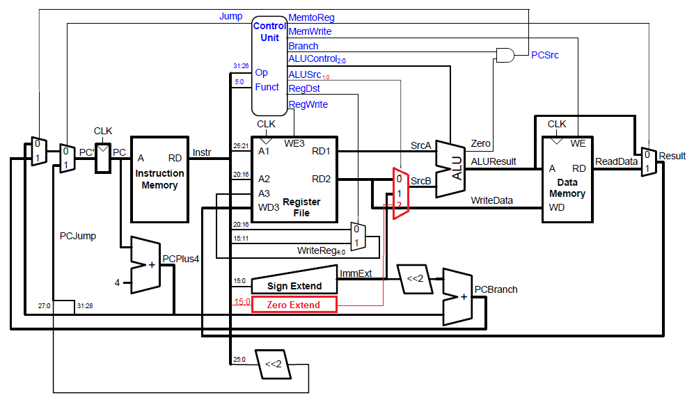
A new component "zero extender" had to be made since for a bitwise OR operation, the operands have to be the same length. With the ORI operation a register value is being ORd with an immediate and in the MIPS archetecture a register value is 32 bits and an immediate is 16, for the ORI to work the 16 bit immediate had to be "padded" with 16 more zeros, the zero extender accomplishes this task.
The ALU's multiplexor had to be changed to a 3 selection mux becasue if an ORI is going to happen the 32 bit immediate had to be used. Since the mux became a 3 selection there would have to be a 2 bit selection signal to choose, ALUSrc needed to be 2 bits.
####Decoder Tables The tables for the ALU decoder and the main decoder were then updated to account for the new instruction. ORI has an opcode of 13 and is ver similar to addi since it is an immediate instruciton that completes an arithmatic operation.
######Main Decoder
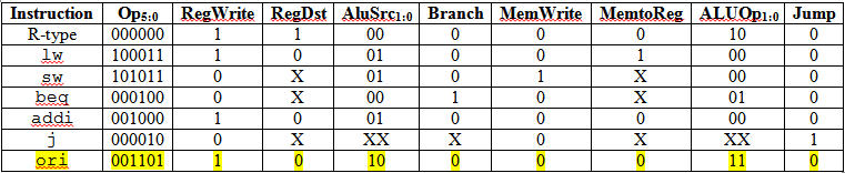 the new instruction can be seen highlighted at the bottom
######ALU Decoder
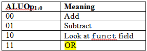
The ALU should preform an OR operation which already exists in the ALU.
####VHDL Modifications In order to implement the new schematic in VHDL the two new components had to be made. The zero extendor was created using the sign extender as a template. Its behavior was as follows
architecture behave of zeroext is
begin
  y <= X"0000" & a;
end;
the 3 selction mux was created using the 2 selection mux as a template
architecture behave of mux3 is
begin
  y <= d0 when s = "00" else		--0 selection
		 d1 when s = "01" else		--1 selection
		 d2 when s = "10";			--2 selection
end;
it is important to note that after the mux was created the signal ALUSrc had to be changed to be 2 bits to account for the third selection. This ment changing the signal decleration in all 13 spots. Once the signal declerations were changed the port map in each components decleration had to be changed to reflect the new order of signals.
#####Simulation
The instuction ori $S3, $S2, x8000 was converted to its machine code (0x36538000) using the same process as preciously outlined. It was put into the testbench as follows
--ori $S3, $S2, x8000
		instr <= X"36538000";
		wait for clk_period;
When simulated the following waveform was generated.
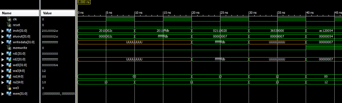 When 7 is ORd with 8000 the expected result would be 8007 which is what appears in the aluout signal after the operation is run indicating a sucessfull implementaion of the ORI operation
##Documentation C3C Spence helped me realize that I had to rename all of the alusrc signals so they were 2 bits. He also compared machine code values to ensure we reached the same answer
C3C Hayden gave me an overall idea of what needed to be changed. He helped me realize that a zero extender was needed and advised me to implement the three selection mux rather than add another 2 selection mux.